| Tills Palm Pages | http://www.harbaum.org/till/palm |

| Homemade 4MB memory extension for Palm III |


This page describes the modification of the old Palm III memory boards. The newer boards contain only one 16MBit DRAM instead of four 4MBit PSRAMs like the board described in the mod. You can easily distinguish between both boards on the number of chips on them. The old board required for this mod has a total of five chips on it, four RAMs on one side and a Flash ROM on the other side (the top side if installed in a Palm III). This board can be upgraded to 4 Megabytes as described in this text. The new board only contains four chips on one side (the bottom side if installed), one chip is the Flash ROM, one a TRG DRAM controller, one a multiplexor from Texas Instruments and one the 16MBit DRAM. If you have this board you can't upgrade it to 4 Megabytes, but you can upgrade it to 8 Megabytes! You can also distinguish between the boards without even opening the pilot just by starting my meminfo application (only for non-EZ machines, e.g. Pilot, Palm III). If it finds two RAM banks with 2 MBytes each (the second bank is in fact empty, but PalmOS enables it, anyway) you have a new board. If it shows two banks with 1 MByte each you have the old board required for this mod.
| What's this all about? |
|
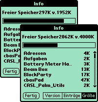
These instructions will show you how to build a memory extension for your Palm Pilot. This modification requires you to open your Palm Pilot and, therefore, voids the warranty of your Pilot. In opposite to the 1MB and 2MB RAM extensions for older Pilots these modifications are not based on an extendable memory board design. This modification is really difficult to apply and requires advanced soldering skills, since this is all very small SMD stuff. You'll need to solder small wires to pins with a width of about 0.3 mm and 0.35 mm space to the next pin. And now for the good thing: With this modification your Palm will have as much as 4MB RAM. This modification requires no modification of the Palm-OS or hacks or drivers to work. The additional memory will just be recognized by the OS as you see in figure 1 (these are snapshots from my (German) Palm III before and after the modification). |
|
Additional disadvantages of this circuit are a worse RAM timing. Due to some additional parts we've to integrate into the RAM decoding process, the RAM access time gets shorter (about 5 to 10ns). I can't guarantee, that this will work with your pilot. But if your pilot can be run at more than 16 MHz, it will most likely work with slower RAM access at 16MHz. Furthermore, the Pilots were designed to run with 85ns RAM, but todays pilots use 80ns RAM, which gives us 5ns to play around with. I'm using an address decoder with 13ns delay and can still over-clock my pilot to 24MHz, so there seems to be no problem. You should be careful, if your pilot can't be over-clocked. Another problem may arrive due to the increased power consumption. Since my pilot uses rechargeables and has a charger built into the cradle this is no problem for me. Anyway, i've done some measurements with the modified and the unmodified pilot. The power consumption in running mode is increased from 17mA to 21mA. Battery life will be shorter by that factor. |
| How does this work? |
|
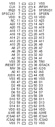
The pilots memory is directly attached to the DragonBall processor, which is the all in one chip, that drives your pilot. To understand the following description you should read the data sheet for the DragonBall. One part of this chip is a programmable address decoder which manages the access to the RAM and Flash ROM in the pilot. The DragonBall (with a little help of a small custom chip, we'll come later to) uses six control signals to select the different memory chips. The pilot uses the CSA0 pin to access the ROM (or Flash ROM) containing its operating system (cf., figure 2). In the Palm III it is programmed by the OS to decode an area of 2MB ROM for this chip. With the older (1MB and less) ROMs, this pin is programmed to decode 1MB. The Palm-OS3 maps the area decoded by this pin to the address area from $10c00000 to $10dfffff. A second pin (CSA2) is programmed to map some other hardware to the address area from $10e00000 to $10ffffff. This pin seems to be programmed to access a second ROM chip allowing an overall ROM area of 4MB. In fact the memory board of the Palm III has spare solder contacts which are identical and next to the place where the OS ROM is soldered (cf., figure 11). | 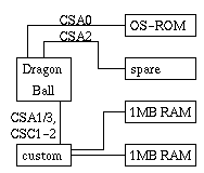
|
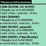 |
The 2MB RAM of the Palm III are accessed with the CSA1 and CSA3 lines. These lines are not directly attached to the memory chips, but are wired to a custom chip (U51) which is itself connected to the memory. One reason for this is, that the RAM timing (in opposite to the ROM timing) is not generated internally by the DragonBall, but externally by U51 (external dtack). Figure 3 shows the output of my Memory Info application (source) which displays the current state of the CSAX signals (the addresses are displayed without the group register offset which maps all addresses to the $10xxxxxx area). As you see in figure 3 all select signals are programmed as 'read only'. This is where CSC0 and CSC1 enter the stage. These signals are combined with CSA1 to generate the chip select signal for RAM bank 0. This bank contains 1 MB of the 2MB of the Palm III (in machines with 1MB or less this is the only bank available). CSCX are simply 'or-ed' to CSA1 and they are programmed to map the first 96 kBytes (64k with Palm-OS2) to address 0 in read/write mode. The second RAM bank (1MB at Palm III and empty in all other machines) is mapped via CSA3 to succeed RAM bank 0. Again: All RAM is mapped to address $10000000 read only (starting with bank 0 followed by bank 1). The first 96k of bank 0 are additionally mapped to address 0 for read/write access. |
|
You'll ask 'What is this good for?' The answer is simply: Memory protection. Since the DragonBall does not have a memory management unit, USR chose this clever way to give the running program a 96k RAM area to work with, but prevent it from writing to the code/data area of other applications. The remaining RAM area is used to store programs and databases. But how do these programs get there if you can't write to it? The Palm-OS enables write accesses to this area during hotsync or updates of a database. There are undocumented OS functions (MemSemaphoreReserve and MemSemaphoreRelease) for enabling and disabling write access to the whole RAM area, but you should never use these functions, since you can erase/destroy the whole RAM area with this. |
|
Additional RAM can be added by extending the RAM area, decoded on the memory module. Palm-OS first enables the first RAM bank (bank 0) and checks its size. Once it determined the size of this bank it programs the second bank (bank 1) to succeed bank 0. If you increase the size of bank 0, bank 1 is mapped behind the increased area of bank 0. You can see this when playing around with the xcopilot emulator and my meminfo application. The emulator only uses bank 0. Independent from the size, you choose for the first bank, a second bank is enabled behind the first one addressing the same size of memory (even if this second bank contains no RAM at all). The Palm-OS then runs a memory check to determine the correct memory size. Figure 4 shows my program running on my modified Palm III with a RAM bank 0 of 4MB and a RAM bank 1 containing no RAM at all. You see both areas programmed to 4MB and the second one mapped to directly succeed the first one. One thing you should not do is to extend the second bank to contain more RAM than the first one. Since Palm-OS programs the second bank the same size as the first one, it'll not be able to access the additional RAM. | 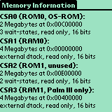
|
| OK, i want 4MB, how do i do this? |
 |
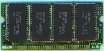
Just by extending the RAM banks :-) I've done this by soldering a second layer of RAM chips directly on top of the old ones. In figure 5 you see one RAM and another one soldered on top of it. |
|
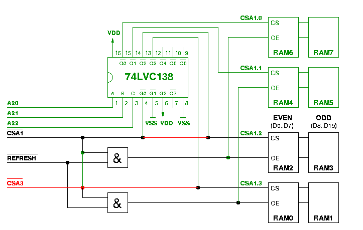
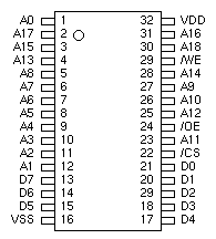
Of course you can't solder all pins directly to the pins of the bottom RAM. You need to select the old chips for one memory area and the new ones for another one. Figure 6 (click for a larger version) shows the schematic of my modification. Red connections are connections to be removed, green ones are new and black ones are the remaining connections. The new RAM chips and the old ones are selected via the CS signal (cf., figure 8). The RAM chips are accessed in pairs (giving a 16 bit bus with 8 bit wide RAMs). According to figure 10 the first and the third RAM chip are the pair for bank 0 and the second and the fourth chip (from left to right) are bank 1. Now you have to unsolder pin 22 (/CS) of all original RAM chips from the board and lift them carefully of the board. |
 |
|
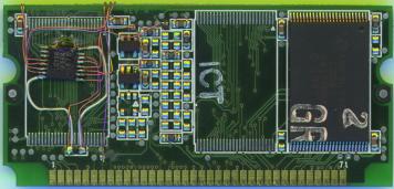
Now connect pin 22 of the left RAM and pin 22 of the third RAM with a thin wire and leave a short part of this wire free to connect it later on the other side of the board. Do the same with pin 22 of the second and the fourth RAM, again leaving a short part of the wire unconnected. You can see these wires in figure 10 between RAM three and four and right to RAM four going to the other side. Now solder the new RAMs on top of the old ones by bending the pins (except pin 22) of the new ones carefully down. Be sure to put them as close together as possible, because the RAMs have to fit between the memory module and the motherboard of the Palm III. Bend pin 22 up a little bit and again solder a wire to the first and the third RAM and to the second and fourth one. Again, leave an end to connect later to the other side of the board. Now you are done on the RAM side of the board, leaving 4 wires to connect somewhere on the other side. This is where some new logic will be placed. This logic has to split accesses, that went to the old RAMs into different access signals for the old and the new ones. This is done by a 3 to 8 decoder (74LVC138). You really need a low power 3.3 V type, like the 74LVC138 (6.7 ns delay) from Texas Instruments (or the 74LC138 (13 ns delay) from TI or the 74LCX138(6ns)/74LVX138(6.7ns) from Motorola or the 74LVQ138 (5.5 ns) from Thompson). This chip now includes additional address lines into the chip select signals. It can easily be glued to the memory module as shown in figure 11. VDD and VSS can be wired to some unused pads on the board (the white wires in figure 11 are VSS and VDD). Two of the enable signals (G1 and G2) of the 138 have to be tied to VSS and VDD, too, since they are unused in this circuit. The old CSA1 signal is accessible at pin 1 of the upper one of the small and-gates in figure 11 and has to be connected to the remaining enable input (G0) of the LVC138. This gate includes a refresh signal into the generation of OE, since these are pseudo static RAMs and need refreshing. The additional address lines (A20 - A22) are all available on small test pads on the board and need to be connected to input A to C of the 74LVC138 (pins 1 to 3). The new select signals are now available at pin O0 to O7 of the LVC138, giving eight decoded areas of 1MB for bank 0. Since these are sufficient for our 4MB project, we don't need to solder in a second decoder to extend the second bank. Instead we connect all 4MB to the first bank, even those, that were formerly connected to bank 1. |
|
|
Now that all memories are mapped to bank 0, the /OE signal for the RAMs of the old bank 1 has to be generated via CSA1 and RFSH instead of CSA3 and RFSH. This can be achieved by disconnecting pin 1 of the second gate (the lower one in figure 11) from the PCB and connect it with a little wire to CSA1 which is available at pin 1 (cf., figure 9) of the upper gate. Now all /OE signals are driven by CSA1. You now have to connect the four CS wires from the RAM side of the PCB to the first four decoded outputs of the LVC138 (O0 to O3). Voila, we are done. Take a close look at all connections (especially the wires soldered to pin 22 of the RAMs). Put the memory module back to your pilot and enjoy!!! |
| What about even more RAM? |
|
Yes, this seems to be possible. With our circuit it is possible to drive 8MB in one bank. With an unmodified second bank this gives you 9MB. Tests with the emulator show, that Palm-OS is capable of handling 12MB RAM. This can't be done by adding more RAMs on top of the old ones, since the RAMs have to fit between the memory card and the motherboard. There's no room for more RAM. Another problem may be the additional load to the address lines of the DragonBall. |
|
|
I'm quite sure, that it is possible to use a memory size which is a power of two (like 1MB, 2MB and 4MB) with one bank. And this must be so if you want to use RAM on the second bank, too (since it's otherwise impossible to map both banks without gap). But i don't know, if it's possible, to increase the first bank to odd amounts like 5 or 6MB. But this is likely to be possible. |
Although this circuit was developed for the Palm III, it can be added to a Palm-OS3 upgrade board and even to already upgraded Palm-Pro boards. I've not done this and I'm not going to, but it will sure work. Upgrading to more than 4MB may be easier with these boards because the RAMs are not all on the bottom side at these boards, like they are in the Palm III board. With these boards it should be possible, to add a third and fourth layer of RAM on the two RAMs placed on the upper side.
I've unsoldered my RAMs from old Palm-Pro boards. It cost me about DM 90 ($50), which is about 13% of a new Palm III in Germany today. I think this is a good alternative to other 8MB upgrade boards, which cost as much as a new Palm III. |
 |
| Tills Palm Pages | Get in touch! |