
The SPI2CF CPLD design
The SPI2CF chip used in the SPI2CF demo system is based upon a cheap CPLD. The necessary WebPack ISE development system is available as a free download from Xilinx. It can therefore be used for homebrew projects. The chip used is the XC9572XL CPLD which is being used to interface the CF card with the SPI interface of a host CPU.
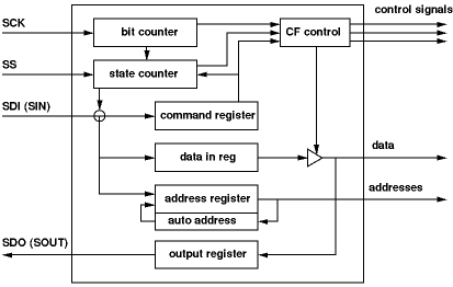
In order to have the chip homebrew friendly the PLCC44 package was chosen which can even be used on a breadboard with the appropriate socket. The downside of this choice is the fact that the package only has 44 pins of which only 34 are available to the user. The remaining ten pins are needed to supply power to the chip and to be able to program it. Fortunately a SPI interface only needs 4 pins (SCK, SDI, SDO and SS) which also saves pins on the CPU it is being connected to. This leaves 30 pins for the CF interface. The CF interface uses 11 address lines and at least six access control signals (CE, REG, OE, WE, IORD and IOWR). This leaves less than 16 pins and thus doesn't allow for a 16 bit CF interface. Instead the SPI2CF interface only uses 8 data bits to transfer data from and to the CF card. This isn't really a limitation since the SPI interface is the limiting factor and switching from 8 to 16 bit on the CF side wouldn't increase the performance. The SPI interface was inteded to run at most at 10 MBit/s on a AVR cpu running at 20Mhz. The goal therefore was to be able to have the chip actually cope with this max. SPI data rate.
Transferring a byte via SPI at 10Mhz takes 800ns. The CF cards slowest transfer modes are allowed to take at most 300ns which means that the CF interface can easily cope with the SPI interfaces speed.
An access is always initiated by the CPU via SPI. The start of a new access is indicated by the SS signal going high for some nanoseconds. This resets the internal state machine and bit counter and causes the chip to expect to receive a new command byte. The CF access itself is then done autonomously by the SPI2CF chip while pure software based CF drivers have to generate the complete CF timing in software. The SPI2CF chip thus massively helps the CPU in driving the CF slot and at the same time increased the reliability due to the very exact timing possible with the CPLD.
The serial peripherial interface (SPI) is a synchronous serial interface. It uses a clock line and a seperate data in- and output connection which are used to transfer bytes one bit after the other. A fourth signal often named SS may be used to select a certain spi target and/or to synchronize the SPI transfer. The exact usage of this helper signal varies from application to application.
The interesting part of the SPI is that it always transfers data in both directions. Whenever a byte is being sent another one is received and vice versa. While this is useful in some scenarios it's often not used and one of the two bytes is silently dropped.
The SPI2CF as well uses only one direction at a time most of the time. If e.g. a command byte is being sent from the CPU to the SPI2CF chip the byte being returned at the same time (usually) doesn't contain useful data and is being dropped. On the other side when reading data from the SPI2CF chip a dummy byte of any value has to be sent from the CPU to the SPI2CF and the focus is on the returning byte.
The current version of the SPI2CF chip has been tested to work at 8MHz SPI clock rate. With CF access times garuanteed to not take longer than 300ns up to 10MHz SPI rate should work. Unfortunately tests with 8MHz have not been successful.
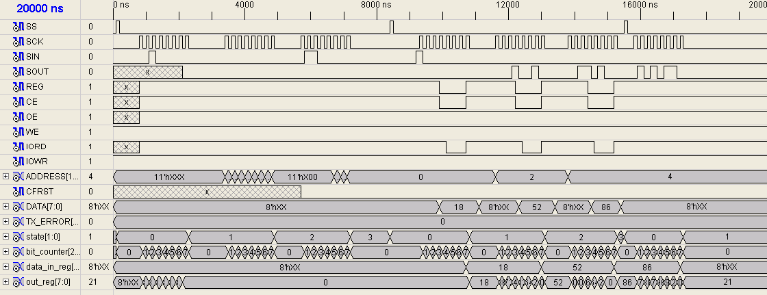
The example above shows the io read access. The first three SPI clock sequences represen the SET_ADDR command together with the 16 address bits which are uploaded to the CPLD. The last four sequences are the IO_READ command incl. the last byte being transferred during a "fake" GET_ID command phase. This prevents that another byte is being read from CF while the last byte is forwarded via SPI.
Only 3 of the 8 command bits are actually used. The valid commands are:
| command | 3 bit code | byte code | Description |
|---|---|---|---|
| GET_ID | 000 | 0x00 | Read the 16 bit chip id |
| SET_ADDR | 001 | 0x20 | Load the 16 bit address latch |
| REG_READ | 010 | 0x40 | Read the CF attribute space |
| REG_WRITE | 011 | 0x60 | Write the CF attribute space |
| IO_READ | 100 | 0x80 | Read the CF IO space |
| IO_WRITE | 101 | 0xa0 | Write the CF IO space |
| MEM_READ* | 110 | 0xc0 | Read the CF memory space |
| MEM_WRITE* | 111 | 0xe0 | Write the CF memory space |
Using only the first three bits had an advantage in the first version of the chip: The chip already knew what to do after these three bits and could fulfil some task in the unused remaining five bit times. If the given command was a read command the chip could therefore do the actual read from the CF card within these five bit slot and the CPU could immediately start reading the result. Thus the byte read from the CF card while the command was received was transferred in the second spi transmission. This can easily be seen in the timing example above. The first IO read access already takes place (CE goes low) while the IO_READ command byte is still being transferred. The latest version of spi2cf does not use the 5 bit cycle but uses the entire eight bit times. This has the disadvantage that an additional SPI byte has to be transferred before any read operation. But this allowed to double the max SPI clock rate to 8Mhz. Thus the overall performance greatly increased in during that step.
See the file avr/cf.c for the part of the driver software dealing with these internals of the SPI2CF chip.
The entire chip design is available as part of the SPI2CF project and is licensed under the GPL. It was designed in the verilog language. A VHDL version is not available.
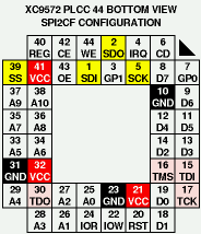
Below is the pinout of the SPI2CF chip as seen from the bottom of the PLCC44 socket to ease development and debugging (thanks to Thomas Fischl for that idea ...). The black triangle represents the rounded edge at the chip.
See the download section of the SPI2CF demo project for the source code.
| Home | Till Harbaum <Till@Harbaum.org> |